 Isaiminia World Breaking News & Top Stories
Introduction:
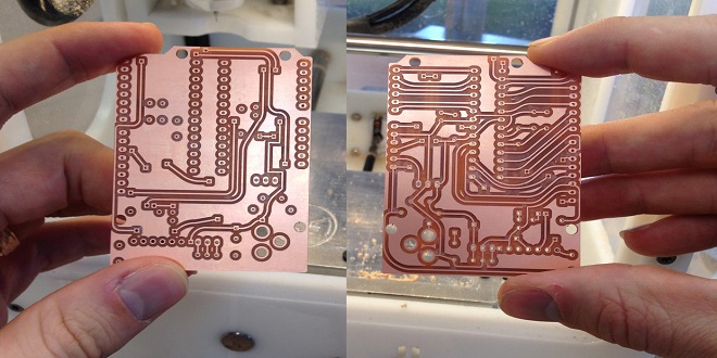
Double sided printed circuit boards (PCBs) have grown in popularity as the need for efficient and compact circuitry has increased in the constantly changing field of electronics. Designers can fit more functionality into a smaller area thanks to these adaptable boards. You’ve come to the correct site if you’re interested in learning how these complex electrical platforms are constructed. In this tutorial, we’ll go in-depth on how to make a Double Sided PCB Assembly from the original design to the finished result. Understanding the manufacturing process behind Double sided PCBs may open doors to a variety of options, whether you’re a hobbyist or a professional in the area.
Getting to Know Double sided PCBs:
Circuit boards known as Double sided PCBs include copper traces on both sides, enabling more intricate and compact designs. They are extensively used in many electrical products, including anything from cell phones to medical equipment. They are widely sought-after for contemporary electronics since they can fit more components in a smaller area.
How to Create a Double sided PCB:
Designing a Double sided PCB thoughtfully is the first step in the process. You’ll draw a schematic design of your circuit using specialist software, such as Eagle or Altium Designer. This diagram serves as a guide for how the connections between the parts should be made.
Getting the Supplies and Equipment Ready:
Once your design is finished, it’s time to acquire the required supplies and machinery. For the PCB manufacturing procedure, you’ll need a copper-clad board, an etching solution, a UV exposure unit, a solder mask, and several chemicals.
PCB layout creation:
It’s essential to convert your design into a physical layout. Components and traces are positioned on the board according to the arrangement. Signal integrity and noise reduction are two important considerations.
Making the Circuit Print:
After the plan is complete, the copper-clad board must be printed with the circuit. A photographic technique is often used for this, in which the design is transferred to the board using UV light and a photosensitive film.
Making Copper Traces via Etching:
Chemical etching eliminates extra copper from the board while preserving the necessary copper traces. The electrical paths are made by etching away the portions that were not shielded by the ink from the previous stage.
Adding Vias and Drilling Holes
For through-hole components and vias—connections between the top and bottom copper layers—drill holes are necessary. Traces may go through vias, which improves the board’s connection.
How to Use a Solder Mask:
To protect the copper traces on the board and avoid solder bridges while soldering the components, a solder mask is placed. Your PCB will be more protected after this process.
Conclusion:
A fascinating fusion of art and science is needed to create a Double sided PCB. The result of the rigorous design, exact manufacture, and expert assembly is a useful piece of technology. With the information from this thorough manual, you’ll be better prepared to realize your electrical ideas as you explore the realm of PCB design. Remember that these complex circuit boards—the foundation of contemporary electronics—are responsible for a portion of the functioning of any gadget you use.
Here check about more details on pcbasic.